Next Generation IC Chip Manufacturing Technology at IIT Mandi, 22 June
Integrated Circuit (IC) devices play an indispensable role in modern society, from industrial applications such as computer controlled and operated machinery to mechtronics, telecommunication, and daily computing needs. In this endeavor, researchers at IIT Mandi recently designed and developed certain fabrication and manufacturing methods for ICs that overcome many of the inherent problems present in the current methods.
In today’s world, semiconductor chips play a vital role in day-to-day life by making our life pleasurable, safer, and healthier.As semiconductor-device manufacturers compete to offer high performing, low-heat generating, and cost-effective devices, there has been a continuous drive to reduce the IC-feature sizes. Reducing the size of features boost speed and improves the economics of manufacturing by allowing more transistors (often more than 50 million) to be placed on a single chip. The radical improvements in IC performance stem primarily due to the interconnection of millions of active components such as transistors and diodes on a single silicon chip.The smallest components on a chip are transistors (basically these are switches), and there can be billions of such transistors on a chip. Together these transistors perform faster computing and contain memories that collate huge amounts of data. In addition, reducing the chip size is important as small-sized chips are less costly to manufacture.
According to the International Semiconductor Roadmap, the technology that enables one to print finer features on chips is (nano) lithography, which historically follows the renowned Moore’s Law for IC-miniaturization. From the beginning, photo lithography tools have been used to enable low cost and high speed transfer of circuit design patterns onto silicon substrates, making mass-manufacturing possible. For example, lithography lays down the foundation for constructing3D IC structures. As the degree of integration of electronic components in ICs increases from a few to hundreds of millions of transistors, the demand on the performance of lithography tools also evolves. With the IC feature-size having already moved towards the 22 nm node and the current 193 nm wavelength, the Deep Ultraviolet Lithography (DUVL) tool sets have reached its potential for further development. Thus, we need some next-generation lithography tools to be used by the industry.
Among the potential next-generation tools(e.g., Extreme ultraviolet lithography (EUVL), EB, X-ray and nano-imprinting technologies), it is expected that EUVL at 13.5 nm wavelength has good prospects of being adopted for high volume production in the near future. In addition, compared to DUVL-based technology, EUVL has two major advantages. Firstly,it is cost-effective,has higher unit throughput, and a simplified working. Secondly, it could be extended to realize even smaller feature sizes (16nm or 10nm). Therefore, it is anticipated that EUVL will become a major technology for next-generation IC fabrication and manufacturing.
However, current implementations of EUV lithography faces several challenges including that of finding photoresists that can concurrently achieve narrow line width around 16 nm, small line edge roughness at 3σ (1.5nm), and high photo sensitivity at 2-10mJ/cm2. Prof. Kenneth Gonsalves, Visiting Distinguished Professor, IIT Mandi, developed a unique strategy to deal with key problems causing the technical deficiencies in the current EUV photo resist technology. He successfully demonstrated the feasibility of developing a EUV photo resist with high sensitivity, high resolution, and low-line roughness.
The current project at IIT Mandi encompasses the design and development of resists that are directly sensitive to photons without utilizing the concept of chemical amplification (CARs) and addresses many of the inherent problems of currently used chemically amplified resist technology (e.g., acid diffusion, sensitivity, post exposure instability). The newly developed resist materials, while highly sensitive to photons of various wavelengths, function as non-chemically amplified resists. This new resist design is accomplished by polymers that are prepared from monomers containing sulfonium groups.
In order for a polymer to be directly sensitive to exposures at the 13.5 nm wavelength, a highly sensitive group must be introduced into the polymer units. Sulfonium groups have been found to be sensitive to UV photons. For this reason, sulfonium groups have been chosen as photon sensitive groups in non-CA resists. In the development of this technology, Prof. Gonsalves discovered that polymers prepared from monomers containing sulfonium components are highly sensitive to DUV photons and act as non-chemically amplified (non-CA) negative resist materials. It was also observed that these non-CA resists are sensitive to e-beam irradiation and would therefore be useful for EUVL down to the 16 nm node and below.
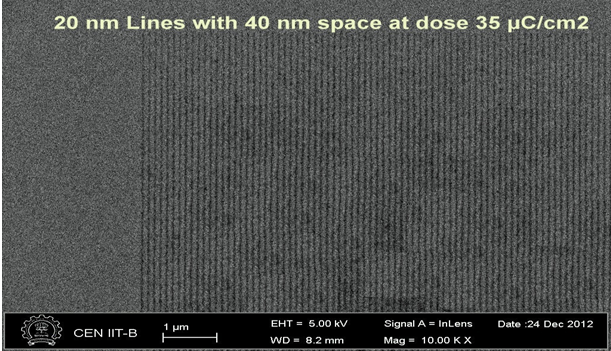
At IIT Mandi, working with an interdisciplinary team comprising of chemists, material scientists, and electronics engineers, Prof. Gonsalves has been currently developing new non-chemically amplified resists of sizes 16 nm to 10 nm node. In this program,the research team has successfully developed and tested resists that show resolution at 20 nm under electron-beam exposures. Having shown the proof-of-concept in the first year of the project, these prototypes will now be tested for imaging at the 16 nm and lower node under EUV exposure in the second year.In addition, additional hybrid organic–inorganic resists that achieve 16 nm node sizes are in the pipeline.
The project team is headed at IIT Mandi by Prof.Gonsalves as the principal investigator. Additional co-PIs at IIT Mandi are Assistant Professors: Dr. Subrata Ghosh, Dr. Pradeep Parameswaran, School of Basic Sciences; and, Dr. Satinder Sharma School of Computing and Electrical Engineering. The Postdoctoral research Fellows on the project are: Dr. V. S. V. Satyanarayana, Dr. Vikram Singh Tomar, and Dr. Vishwanath Kalyani.
IIT Mandi acknowledges financial support for this project by Intel Corp USA administered through the Semiconductor Research Corp (SRC) USA.Also, IIT Mandi acknowledges use of facilities at INUP Mumbai.
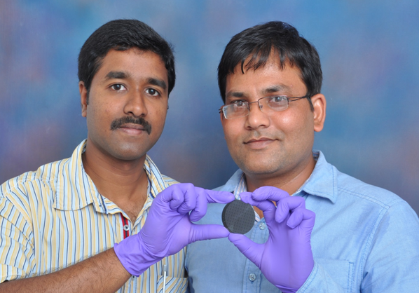 |
| Figure 1. Silicon wafer with 20nm lithography patterns obtained by electron-beam exposure. The silicon wafer was fabricated by Dr. Vikram Singh Tomar and Dr. V. S. V Satyanarayana |
 |
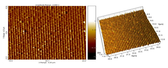
| Figure 2. The 2- and 3- D Atomic Force Microscope (AFM) images of 20 nm lines on silicon |
 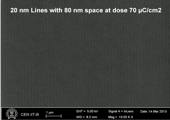 |
| Figure 3. The 20 nm lines pattern in non-chemically amplified resists synthesized at IIT-Mandi, India. This pattern was under the development of new non-chemically amplified resists that attained sizes of 16 nm to 10 nm. |